
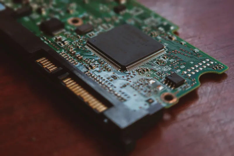
The insatiable demand for artificial intelligence processing power has shifted the semiconductor industry's center of gravity. For decades, the primary metric of progress was shrinking transistors on a wafer using extreme ultraviolet lithography. Today, scaling individual chips has hit physical and economic walls. Silicon designers are instead looking upward and outward, turning advanced packaging into the most critical battleground in tech supply chains.
Advanced packaging involves integrating multiple specialized components—such as logic dies, high-bandwidth memory, and I/O controllers—into a single cohesive system using 2.5D and 3D architectures. Companies like TSMC, Intel, and Samsung are pouring billions into specialized packaging foundries. Without these sophisticated interconnects, top-tier AI accelerators would suffer from severe data bottlenecks, rendering raw computing power largely useless against massive machine learning workloads.
Supply constraints for packaging equipment and facilities are already rippling through the global technology ecosystem. Major cloud providers and hardware startups alike find themselves waiting months for finished silicon, not because the raw wafers are missing, but due to a severe shortage of advanced packaging capacity. This pinch highlights a broader reality for the industry: building the future of artificial intelligence requires rethinking physical assembly just as much as architectural design.





Comments